CHROIX  ·  CUTAWAY
№ 01⤫ CROSSOVER: STRATA2026·06
Issue 01 · The Anchor Object

We cut open theNvidia B200

One GPU, traced from the data center to the mine — and a map of where its value actually hides.

THE CUTAWAY  free
what it is & how it works
THE KEY  paid
where the value actually sits
COLD OPEN

It costs Nvidia roughly $6,400 to build a B200. It sells for around $40,000. That gap is the most-discussed number in technology — and it's the wrong number to be amazed by. Almost none of that $6,400 is the "chip" you picture. The silicon brain is the cheap part. The expensive, fragile, geopolitically radioactive parts are the memory beside it and the packaging that glues it together — and both funnel through a handful of buildings on two islands.

LAYER 01

The Object

01 / 09 — THE DESCENT
8× HBM3e  ·  2 COMPUTE DIES — TSMC 4NP  ·  Si INTERPOSER — CoWoS-L  ·  ORGANIC SUBSTRATE  ·  BASEPLATE
▱ The Cutaway — free

The B200 is the flagship data-center GPU of Nvidia's Blackwell architecture. One module pairs two reticle-sized dies joined by a 10 TB/s link so they act as a single chip — ≈208 billion transistors, ~2.6× the H100 — built on TSMC's 4NP node, with 192 GB of HBM3e across 8 stacks, drawing 1,000 W.

It is not a monolith; it is an assembly — bonded onto a silicon interposer with TSMC's CoWoS-L packaging, the step that quietly governs how many of these can exist at all.

Data Spine

transistors208 B
nodeTSMC 4NP
memory192 GB HBM3e
TDP1,000 W
build cost~$6,400
sticker~$40,000
methodmodeled
▰ The Key — paid

The object you can point to is the least defensible thing in the box. Nvidia designs the logic and owns the software moat — but the module is an assembly of other people's hard-to-make parts, and the real leverage sits a layer down. Hold one question the whole way: if this part vanished tomorrow, could anyone else make it at volume?

What we're tracking this issue: advanced-packaging capacity, lead-time drift past 50 weeks, and whether the memory share ever cracks…
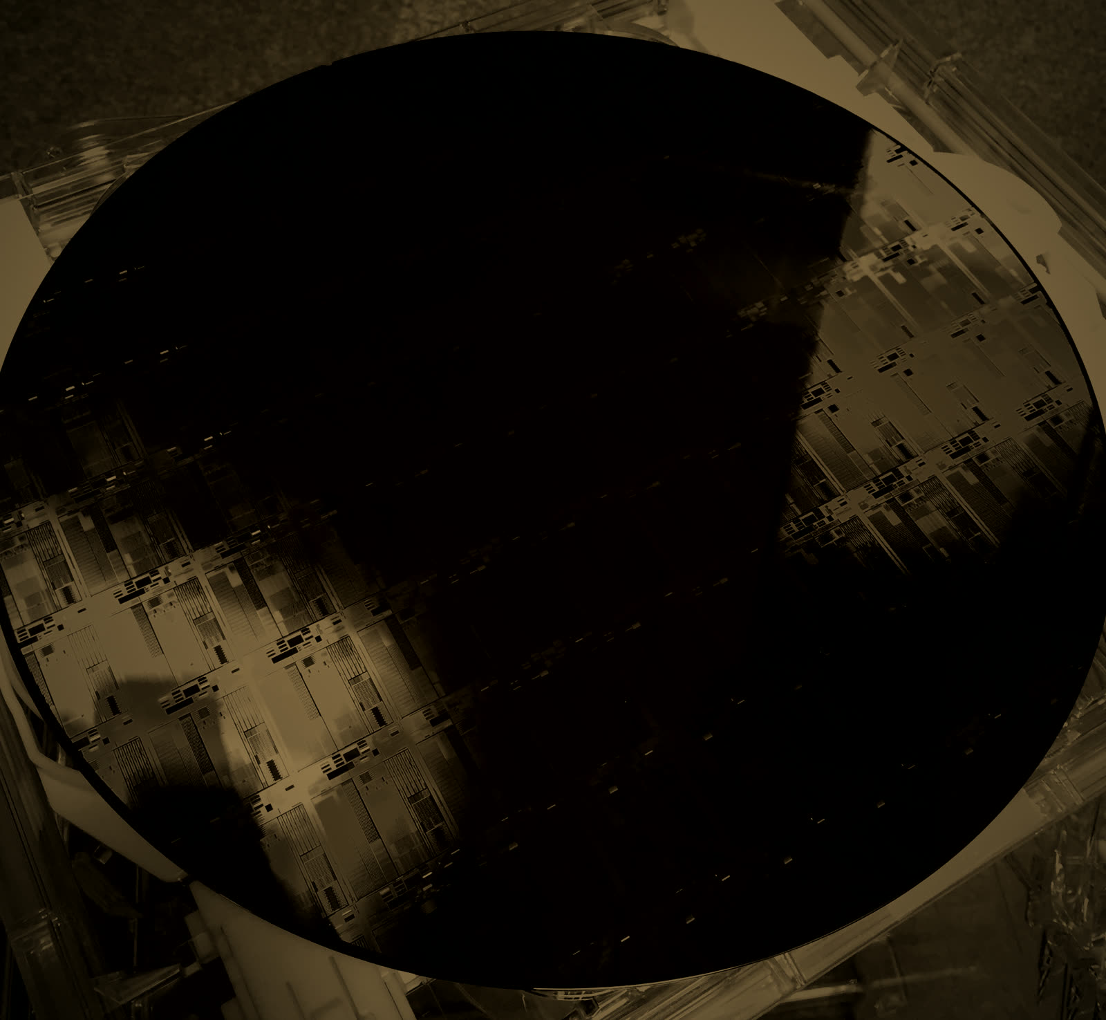
The Key — subscriber read
The teardown is free. The read — where the value hides and what we're tracking — is for subscribers.
Unlock the read →
LAYER 02

The Assembly

02 / 09
LID / HEAT SPREADER
2 COMPUTE DIES + 8× HBM
SILICON INTERPOSER — CoWoS-L · the chokepoint
ORGANIC SUBSTRATE
Signature graphic — THE ASSEMBLY STACK (schematic stand-in)
▱ The Cutaway — free

A B200 is not a monolith; it's an assembly — the single most important fact about a modern chip. Dies and memory are bonded to a silicon interposer, mounted on a substrate, capped, and tested. Without that packaging step, a Blackwell GPU is a pile of loose dies, not a product. The dies come out of the fab and then wait in line to be assembled — backend packaging, once an afterthought, is now the gate.
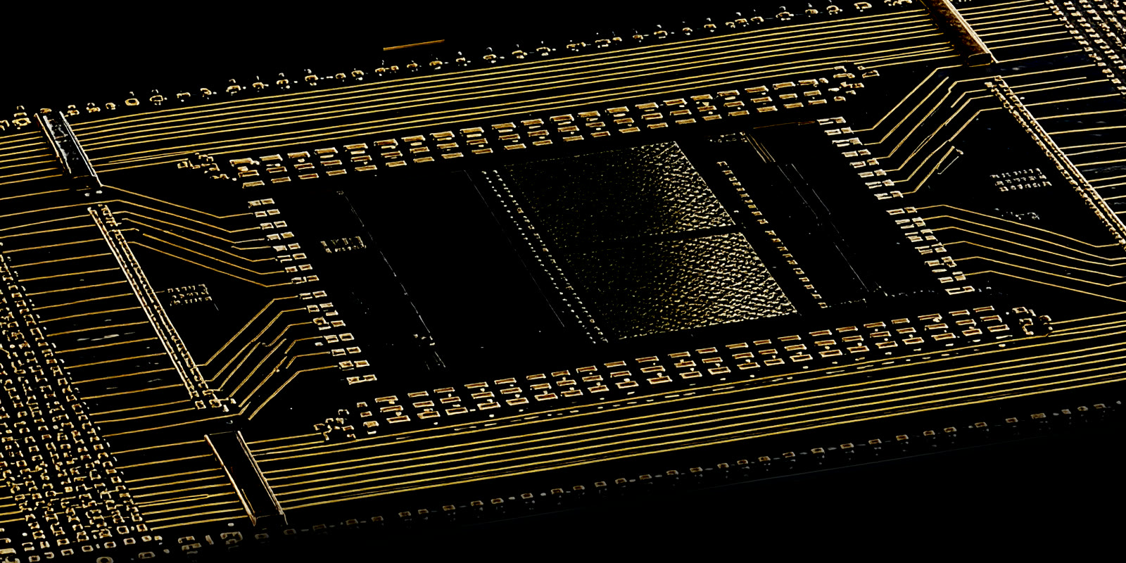
▰ THE KEYThe market narrates this as a fabrication story. It's a packaging story — and packaging is a smaller, more concentrated set of buildings than fabs…🔒 Unlock →
LAYER 03

The Components

03 / 09
TSMC — logicTaiwan · ~90% leading edge SK Hynix — HBMKorea · ~90% of Nvidia's HBM (to date) Micron — HBMUS · #2 Samsung — HBMKorea · #3 TSMC / ASE / Amkorpackaging · TW / US B200 MODULE Nearly every critical edge → Taiwan / Korea. Memory: oligopoly of 3. Logic: monopoly of 1. Taiwan Korea US edge width = supply share
THE SUPPLIER GRAPH — who makes each piece · edge width = share · brass = single-point dependency
▱ The Cutaway — free

Pull the assembly apart and you get a who-makes-each-piece graph that spans the globe: logic dies fabbed by TSMC (~90% of leading-edge), HBM3e ~90% from SK Hynix with Micron and Samsung behind, advanced packaging at TSMC with ASE/Amkor as added OSAT capacity. The punchline: nearly every critical edge terminates in Taiwan or South Korea.

▰ THE KEYMemory is an oligopoly of three; leading-edge logic a monopoly of one; packaging a monopoly-plus-two. The day SK Hynix's ~90% becomes ~70% is a repricing event…🔒 Unlock →
LAYER 04

The Materials

04 / 09 · ↘ STRATA
300mm silicon wafer with patterned dies
THE MATERIALS — a 300 mm silicon wafer: the substrate everything else is patterned onto. Photo: Ehsanshahoseini — CC BY-SA 4.0 (duotone derivative, same license).
SILICON · semiconductorCOPPER · conductor HAFNIUM · dielectricTUNGSTEN · contacts GOLD · packagingTANTALUM · capacitor NEODYMIUM · magnetic
Signature graphic — MATERIAL CLASS MAP (the object re-skinned by matter)
▱ The Cutaway — free

The components dissolve into materials: patterned silicon with copper wiring, hafnium gate dielectrics, tungsten contacts; the package adds gold, tantalum, solder; the board and rack add copper by the kilogram and rare-earth magnets. Materials are where substitutability — the real source of pricing power — gets decided.

▰ THE KEYA part with three suppliers is a negotiation; a material with no substitute is a chokepoint. This layer is the handoff to Strata, which tracks the supply side weekly…🔒 Unlock →
LAYER 05

The Elements

05 / 09
Sisilicon
Gagallium
Gegermanium
Inindium
Asarsenic
Cucopper
Augold · 3TG
Tatantal · 3TG
Wtungs · 3TG
Hfhafnium
Pdpallad.
Ndneodym.
Signature graphic — THE PERIODIC TABLE OF THE B200 · brass = conflict mineral (3TG)
▱ The Cutaway — free

Down to the periodic table — where the object stops being "technology" and becomes extracted earth. Four of these — tin, tantalum, tungsten, gold — are the legally defined conflict minerals (3TG) under Dodd-Frank §1502 and the EU. The GPU is, definitionally, a conflict-mineral product.

▰ THE KEY"No substitute" is the most valuable phrase in this issue. Gallium is the cleanest case — irreplaceable, and a by-product no one mines on purpose…🔒 Unlock →
LAYER 06

The Ground

06 / 09 · ↘ STRATA
Bingham Canyon open-pit copper mine seen from orbit
THE GROUND — Bingham Canyon, Utah: the largest open-pit mine on Earth (~4 km wide, 1.2 km deep), seen from the ISS. NASA / ISS Crew Earth Observations — public domain. Duotone treatment.
PRODUCER SHARE — where it comes out of the ground gallium · China majority △ single-source + export controls (Aug 2023) rare earths · China 60%+ palladium · Russia 34% platinum · S.Africa ~45% THE BY-PRODUCT TRAP Gallium = aluminum by-product. Germanium = zinc by-product. No one mines them on purpose — so "mine more" isn't an option. US 100% IMPORT-RELIANT: arsenic · fluorspar · gallium · germanium · indium · tantalum
THE EXTRACTION MAP — producer concentration + the by-product trap · figures per spec
▱ The Cutaway — free

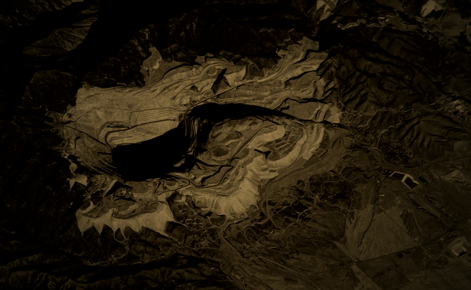
Where the elements come out of the earth — and the brutal concentration of it. China controls the overwhelming majority of refined gallium and imposed export controls in August 2023; gallium is a by-product of aluminum refining, so no one can simply "mine more." The U.S. is 100% import-reliant for arsenic, fluorspar, gallium, germanium, indium, and tantalum.

▰ THE KEYThe by-product trap: you can't fix a gallium shortage by mining gallium. Supply is hostage to aluminum economics and one country's export desk — the Strata seam…🔒 Unlock →
LAYER 07

The Ledger

07 / 09
BOM · ~$6,400 (modeled) HBM ~45% $2,900 LOGIC ~18% CoWoS ~17% chokepoint OTHER ~20% COST → STICKER $40,000 sticker ~84% gross margin $6,400 build
THE DOUBLE LEDGER — what it costs to build vs. what it sells for · Epoch AI, modeled
1,000 W
per B200 in operation
~101 B L
TSMC water · 2023
~15 Mt
TSMC CO₂ · 2020
THE HIDDEN LEDGER — embodied at the fab
▱ The Cutaway — free

HBM + packaging ≈ two-thirds of the cost. The "chip" is the cheap part. Chip-level gross margin is ~82% on Epoch AI's central estimate — and Epoch cautions the realized margin runs lower once it's sold as a rack/server. And the hidden ledger: TSMC alone consumes ~6–8% of Taiwan's electricity and ran on ~101 billion liters of water in 2023.

▰ THE KEYThe margin isn't the thing to track — its inputs are: HBM price (45%, one dominant supplier) and CoWoS price (17%, capacity-locked) are someone else's revenue line…🔒 Unlock →
LAYER 08

The Map

08 / 09 — THE CENTERPIECE
TAIWAN · 2 CHOKEPOINTS, ~100 MI FROM THE MAINLAND NVIDIA · DESIGN (Santa Clara) Arizona dies → ~12,000-mi round trip to TW MINE DRC·CN·RU·ZA REFINE China-dominant TSMC · FAB Taiwan · 4NP ~90% leading edge CoWoS-L Taiwan · packaging the gate SK HYNIX Korea · ~90% HBM ASSEMBLE ODM · TW/MX DATA CENTER US · Gulf · Asia LANDFILL Global South
THE MASTER MAP — one B200's supply circuit, mine → data center → landfill · brass = chokepoint fuse
▱ The Cutaway — free

One B200's journey, mine to data center. Even dies fabbed in TSMC's new Arizona fabs are flown back across the Pacific to Taiwan to be packaged — roughly 7,500 miles each way (Arizona CoWoS isn't online until ~2028). Three single points of failure — TSMC, CoWoS, HBM — two of them on one island 100 miles from mainland China.

▰ THE KEYThe map is a risk model. Every dollar of AI-capex optimism is underwritten by an assumption about two buildings in Taiwan and one in South Korea staying online…🔒 Unlock →
LAYER 09

The Afterlife

09 / 09
Workers salvaging metal from electronic waste, Agbogbloshie, Accra
THE AFTERLIFE — Agbogbloshie, Accra: one of the world's largest e-waste sites, where the metals are recovered by hand. Photo: Marlenenapoli — CC0 (public domain). Duotone treatment.
▱ The Cutaway — free

A data-center GPU lasts ~3–5 years; used H100s already trade at ~$15,000–$28,000. At end of life it becomes e-waste — and a rich ore: a tonne of circuit boards holds on the order of 90–300 g of gold (vs ~1–5 g/t for natural ore) plus ~200 kg of copper. Hydrometallurgy recovers ~95%+ of the copper and ~60–95% of the gold — yet globally only about a third of e-waste's metal value (~$28B of ~$91B in 2022) is actually recaptured; the rest is lost to landfill, incineration, or toxic informal recycling. A GPU is engineered to be nearly impossible to take apart for repair, yet must be taken apart to recover what it's made of.

▰ THE KEYThe depreciation curve is a live signal for how fast "AI capex" becomes "AI write-down." And the fleet is a future ore body with grades above many mines…🔒 Unlock →
B200 package substrate — gold traces and the central die cavity
End of the descent — nine layers, one object. The reading begins.
Part II — The Departments
One Element

Gallium

Irreplaceable, a by-product of aluminum refining, ~100% U.S. import-reliant, and the opening shot of China's 2023 export-control campaign. Tracking: import shares, ex-China projects, price.

Chokepoint

CoWoS

The packaging step that now decides how many AI chips can exist. Nvidia's capacity lock-up + the Arizona-to-Taiwan round trip is the whole story.

Then / Now / Next — the power line
700W
H100
1000W
B200
1400W
B300
HBM4
Rubin ’26
The Substitute

Real vs. vapor

Glass substrates vs. organic; HBM4 and the 16-high stack; Samsung/Micron breaking SK Hynix's grip; the so-far-failed hunt for non-Chinese gallium. What's real, labeled.

Watch List — The Export-Control War
APR 2025The H20 — the deliberately China-capped chip — hit with license requirements; Nvidia takes a $4.5B charge.
DEC 2025Policy opens: the more powerful H200 cleared for China sales, reportedly for a 25% cut of revenue to the US government.
MAY 14 2026~10 Chinese firms (Alibaba, Tencent, ByteDance, JD) approved to buy H200, capped at 75,000 units each — but Beijing froze the deals and not one shipped.
MAY 31 2026Commerce closes the loophole: licenses now required for China/Macau-HQ'd firms regardless of where the affiliate sits. One industry official estimated hundreds of thousands of chips had already routed through hubs like Malaysia. Top-end Blackwell & Rubin stay banned.
Part III — The Data Spine ▰ (every cell carries source + method)
bom — per B200, Epoch AI (modeled, CC-BY)
line_itemcost_usdpctmethod
HBM3e (192 GB, 8 stacks)2,90045modeled
CoWoS-L packaging1,10017modeled
logic dies (2× 4NP)1,15018modeled
total variable mfg6,400100modeled
components — supplier concentration
partsuppliercountryshareconf.
HBM3eSK HynixSouth Korea~90%med
leading-edge logicTSMCTaiwan~90%med
advanced packagingTSMCTaiwanprimarymed
CUTAWAY № 01 — THE NVIDIA B200 A CHROIX PUBLICATION · DESCENT TEMPLATE v0.2 · DRAFT